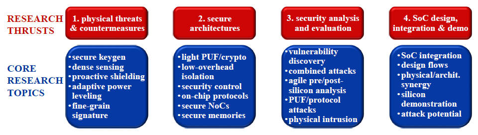
Thrust 1 is focused on establishing a solid ground for the architectural investigation in thrust 2, establishing the trusted computing base (TCB) of physically secure primitives and the root of trust, and protection techniques to counteract physical attacks to the TCB and other attacks leveraging hardware vulnerabilities (e.g., Trojans in IPs, side-channel attacks on IPs and memories).
Thrust 1 will leverage the unique expertise and capabilities of the SOCure team, spanning from secure primitives to physical countermeasures. Among the others, our team members lead the current state of the art in lightweight and low-energy crypto-engines (e.g., AES core with sub-pJ/bit and lowest energy reported to date [ZHA15]), and lightweight Physically Unclonable Functions [AZA16], [JYO17], with the recent demonstration of the first PUF that can is designed in a fully automated manner [TAS17].
Team members have also developed interesting internal capabilities that are currently unavailable on the market, such as a Hierarchy Extractor to analyze the functionality from a flattened gate-level and transistor-level netlist of digital ASIC based on simulation traces, including signal monitoring and observation technique, dynamic specification mining technique and result examples [HE17]. Also, the same group has recently developed an approach(Secure-X) to counteract side-channel attacks with low overhead and high security (unpublished, currently under patent filing). An industrial partner is a worldwide leader in chip imaging and probing for failure and reliability analysis purposes [SEM]. Another industrial partner is a leading company in the field of pre- and post-silicon security evaluation [SIC]. Other industrial partners as silicon manufacturers and design companiesare currently on the process of joining our team. Our international partners from Israel are world-renowned experts in SoC design, side-channel attacks and counteraction techniques [FIS], [KER].
As fundamental basis for the SOCure architecture, a root of trust is needed for each IP to define a different shared secret to encrypt its incoming and outgoing data, and hence enforce strict isolation between IPs. This requires the local generation of a separate key for each IP, preliminary secure key exchange and IP authentication. In turn, this demands the generation of IP-unique ID that cannot be sniffed or tampered with, which excludes the adoption of conventional memories, as they are well known to be vulnerable to a wide range of attacks [KK99]. For example, ROMs are easily reverse-engineered, as the presence of vias on a bitcell indicates the presence or the absence of a transistor at a given address, or through chemical etching when the ROM is programmed via ion implantation. E-fuses are even easier to reverse-engineer via visual optical/SEM inspection or photoemission imaging [T08]. Antifuses can be reverse-engineered via chemical enhancement and Atomic Force Probing Analysis (although slow), photoemission[MSC06], or SEM voltage contrast [Z09], [R02]. Flash memory is also easily readable with SEM for technologies like 0.18μm or older (and in principle Atomic Force Microscope, although very slowly), or via electrical probing.
A fundamentally more secure approach to generate on-chip ID and enable secure authentication is the adoption of Physically Unclonable Function-based ID. As each IP needs an individual PUF, innovation is required to make PUFs ultra-lightweight and easy to design. The first requirement demands the exploration of novel circuit approaches that drastically mitigate the usage of power/area-hungry Error Correcting Codes (ECC), and hence have an order of magnitude better intrinsic stability compared to the PUF state of the art [AZA16]. The second requirement about PUF ease of design translates into the need for PUF architectures that can be designed automatically, which has been recently demonstrated to be feasible by one of our team members [TAS17]. Unfortunately, PUFs generally lack tamper evidence, as fundamental drawback that limits its applicability to secure key generators [NSH13], [TCS06], [PR02]. Hence, novel PUFs with tamper evidence are neededto raise the PUF to the security standards that are required in secure key generation.
In SOCure, innovative lightweight, natively stable and automatically designed PUFswill be investigated to enable their seamless integration as root of trust in the architecture described in thrust 2. Although often ignored in the literature, there is actually a direct relationship between the area/energy penalty of PUFs and their native stability, since the PUF invariably needs to be followed by an Error Correction Code (ECC) block that fixes its unstable bits. The area and the energy is always dominated by the ECC (instead of the PUF), hence lightweight PUFs (inclusive of ECC) need to have adequate native stability, so that the ECC needs to correct only a few bits, and it can hence be made lightweight. As an example, a PUF as in [TAS17] with 256-bit wordlength and a BCH module as ECC adds an area and energy of 350-500 equivalent PUF bitcells, every time an additional unstable bit is added. In other words, the area/energy ECC cost of each additional unstable bit is enormous compared to the PUF itself. Also, the absolute area (energy) cost of a BCH ECC for a typical 10% instability is in the order of 10-20kgates (20 pJ/bit), which is clearly unaffordable when a separate PUF is needed for each IP (its complexity is comparable to a complete ARM Cortex-M0 microcontroller). For this reason, novel PUFs with strong native stability (deep sub-1%) are investigated in SOCure to enable lightweight root of trust. This objective will be pursued by eliminating the large worst-case design margin that is adopted in conventional PUF designs, which covers the worst case process corner, voltage, temperature, on-chip noise and aging factor (see Fig. 9). Actually, it is extremely unlikely that all such worst-case corners will take place at the same time in the same chip, hence the actual instability is much smaller than the worst-case value. Accordingly, novel PUFs able to quantify the design margin and the actual instability at run timewill be explored. The margin and instability will be quantified by measuring the process, voltage and temperature corner with circuits that can sense the corresponding corner. The impact of noise on run-time instability will be instead quantified by embedding low-cost in-situ instability monitors within the PUF bitcells (e.g., current-mode transition detectors). These pieces of information represent features associated with the actual margin and instability, which are inputted to a machine learning engine (e.g., simple decision tree) that estimates the correct number of bits to be stabilized, instead of over-designing the ECC for the worst case.
In SOCure, several uncommon properties of PUFs will be explored to enable unprecedented capabilities that are prohibited by other more conventional ways to store keys (e.g., Flash memory). In particular, in secure SoCs the Flash memory can be erased if chip intrusion is sensed, by simply overwriting the confidential data stored in the memory.However, the attacker can always tamper the chip and promptly disable the supply (or the charge pump employed for write) to preserve the memory contents even if the anti-tampering sensors capture the intrusion, to successfully complete the attack. The attacker can easily stop the erasure since Flash memories require write energy in the order of 1 nJ/bit, which is too large to be stored on chip, and hence needs to come from the external supply. On the other hand, the content of a PUF can be erased or destroyed with an energy in the order of fJ/bit (e.g., developing an on-chip over-voltage through a simple voltage doubler that destroys the oxide of the PUF transistors). Since this energy is about one million times smaller than Flash, it can be stored on chip with small on-chip capacitors with a size in the order of a few μm. This suggests that PUFs can be enhanced with the self-erasure capability by simply storing energy in on-chip capacitors before operating the PUF(see Fig. 10). Then, if an intrusion is sensed, the voltage across on-chip capacitors is used to destroy PUF transistors locally, and complete the erasure even if the attacker disconnects the supply meanwhile (since the energy is pre-acquired on chip). This novel self-erasure property has interesting implications at the application level, as it enables both tamper evidence and remote attestation, as the key integrity provides a proof to a trusted entity of physical integrity of an SoC. These properties are generally prohibited in conventional PUFs, and extend their usage for key generation.
The same above principle to erase PUFs will also be explored to create the novel class of one-time readable PUFs, whose content can be read from the outside only once. This capability solves another limitation of existing PUFs, whose keys need to be read through the chip test port and stored in a secure server before being deployed. The problem lies in the fact that the key can be actually read multiple times by all the players from manufacturing to distribution, which makes PUF keys potentially known to several parties (e.g., assembly, testing house). In other words, conventional PUFs are not able to certify whether they have been illegitimately read previously. In SOCure, the connection of the PUF bitcells to the test port will be automatically blown up after the first PUF read, using circuit techniques that are similar to the above self-erasing PUFs. The self-erasure of the connection to the test port permits to avoid PUF key sniffing during the lifetime of the devices, and to interestingly add read evidence to verify that other players in the supply chain have not tried to maliciously access the PUF. Distributed connections to the test port will be considered to multiply the number of access points that are blown up, in order to make FIB circuit edit unfeasible even if the attacker aims to bypass the disconnection.
As discussed in thrust 2, PUFs will be embedded as building block of trusted routers in the NoC. From a design perspective, this translates into the requirement of low design effort and easy embed-ability of PUFs into digital designs, which can be achieved by enabling fully automated design of PUFs by means of standard cell-based digital design flows. Our team has recently shown the feasibility of automatic design of a specific PUF for the first time [TAS17]. In SOCure, this capability will be systematically explored to design, place and route PUFs along with other digital blocks, achieving immersed-in-logic key generation (see Fig. 11). Among the various advantages, this enables PUF obfuscation within standard-cell designs, as opposed to conventional PUFs that are physically separate on-chip entities, and are hence an easy target for attackers. At further benefit, their design is sped up from months (typical of conventional PUFs) to a day, as was observed in [TAS17].
From the point of view of physical chip security, SOCure aims to introduce innovation to counteract physical attacks, from non-invasive, to semi-invasive and invasive attacks. A wide range of novel techniques will be introduced for truly dense on-chip sensorizationof SoCs, as opposed to conventional approaches that introduce sparse light and laser sensors and can be easily circumvented through imaging or floorplan knowledge. In particular, lightweight laser sensors will be investigated for integration within each standard cell, for ubiquitous detection of laser probing and fault injection attempts. In detail, each standard cell will be equipped with a few properly connected additional sensing transistors that share their diffusions with the transistors implementing the cell, and generate a current when exposed to laser. The output currents of several cells are aggregated hierarchically in current-merging cells that are placed and routed in a fully automated manner, to generate signals that detect intrusion. Interestingly, such hierarchical sensor organization permits to detect both the intrusion and its spatial location, which allows focused and prioritized response depending on which modules are being attacked. Being a largely unaddressed threat, other strategies to counteract laser probing will be explored to achieve a different tradeoff between physical security and area/energy overhead. In particular, in-situ gate-level clock jittering will be explored for the first time to degrade the signal-to-noise ratio of laser probing techniques, and hence quadratically increase the number of averaged acquisitions needed to detect a targeted signal [R11]. Preliminary estimates indicate that 10% jitter (and hence 10% performance degradation) degrades the SNR by ∼10X, which hence increases the attack effort by two orders of magnitude. In-situ gate-level clock jittering will be introduced with fully automated methodologies that can be integrated in digital design flows, based on the insertion of special standard cells with adjustable pseudo-random delay
In addition to dense sensorization, invasive and semi-invasive physical attacks will be counteracted by introducing true spatial randomizationof critical functions, introducing a new level of obfuscation beyond the traditional concept of (deterministic) scrambling. This is achieved by using the above immersed-in-logic PUFs to randomly steer and reorder randomized signals (e.g., through PUF bitcell-based multiplexing). This drastically increases the physical attack complexity, as the localization of a targeted signal requires the physical attack of a large number of spatial location. As representative example of spatial randomization, we will explore the concept of PUF-decoded PUF, where the data PUF address is in turn generated by a content addressable memory (CAM) coupled with another address-associative PUF. This permits to associate an input address to an unpredictable intermediate address that then drives the data PUF, thus making the location of each bitcell unpredictable. The attacker needs to attack a large portion of the PUF (on average half of it), before being able to read a single PUF word, increasing the attack effort and cost substantially compared to the attack of a single well-localized word.
Once laser probing is counteracted, the next most immediate physical threat becomes electrical probing and FIB circuit edit. Traditionally, electrical probing is counteracted by introducing passive and active shielding on top of the chip, using the top metal layers to detect intrusion [LT03], [CDG14], [BCC12]. Passive shielding is well known to be easy to circumvent through FIB circuit edit, as long as the wire replacement has physical properties (e.g., resistance, capacitance) that are not too far from the original properties [CDG14], [SHL], [BCD12]. Active shielding based on the chip side-to-side transmission of encrypted data currently offers the highest degree of security against intrusion from the chip frontside[BR05], [INV], [JE10]. However, a given area can always be penetrated by bypassing the shield wire(s) running onto it by creating a wire detour on top of the external passivation layer (e.g., with RDL layer), so that no interruption is experienced by the shield and hence no intrusion is detected. As innovative research direction, SOCure will investigate the new class of proactive shields, where the top metal layers are used to generate chip-specific keys that are defined by the manufacturing tolerances of these layers (essentially, another PUF). Then, this key is mixed (e.g., XORed) with the keys generated by the more conventional transistor-based PUFs to create the root of trust. In other words, the random variations of shield parasitics are exploited as unique signature of the chip, and they are used as information to be checked at every chip boot to detect circuit edits and intrusions, instead of using other information (e.g., encrypted data) that can always be recreated in a deterministic manner. As interesting implication, the co-generation of keys through the proactive shield and the underlying PUFs leads to a permanent corruption of the keyswhen intrusion form the frontside takes place. This makes the attack pointless, and can also be used as tamper evidence and for remote attestation (i.e., the user can remotely check if the chip has been intruded). Among the other routing options, MOM capacitors will be considered as intrusion sensors, as they are generally laid out automatically in most of commercial design kits. As another interesting implication and advantage over state-of-the-art active shields, the proposed proactive shields do not transmit any ciphertext or plaintext, hence side-channel attacks are completely ineffective and no protection is needed against them.
As opposed to frontside probing, backside electrical probing through FIB circuit edit is broadly acknowledged to be a largely unaddressed threat[CDG14], [HNT13], even when the chip is not thinned down [RHS08]. Accordingly, novel approaches will be introduced in SOCure to counteract backside electrical probing. As first research direction, some unexplored properties of FDSOI will be investigated to create a backside shield. In particular, the FDSOI technology (also manufactured by one of the industrial partners of SOCure) has the unique feature that the diffusion of transistors are not directly accessible from the bulk, due to the presence of the buried oxide layer [PWB12]. In other words, transistors cannot be contacted through backside FIB, leaving the lower metal layers as only option for electrical probing. As unique approach in SOCure, probing of lower metal layers will be prevented by using lower metal layers (e.g., metal 1) as a shield, whereas every transistor is vertically connected to the upper metal layers for routing. This permits to shield the chip from the backside, apply all existing types of frontside protection techniques, and ultimately providing a cohesive solution to the problem of protecting the back side from electrical probing.
Regarding non-invasive attacks, novel solutions will be explored to counteract side-channel attacks at low area/energy overhead, in line with the general goal of SOCure. Indeed, typical solutions to counteract side-channel attacks introduce at least 3X penalty in terms of area and power consumption. Side Channel Attacks (SCA) have been widely employed to expose confidential information (i.e., secret keys) of cryptographic algorithm implementations by correlating the Physical Leakage Information (PLI) and the data processed on chip (e.g., correlation-based attacks). Examples of PLIs are the power consumption, Electromagnetic (EM) emissions, timing and sound generated during the encryption process. Several correlation-based attacks have been demonstrated in the last two decades, including Correlation Power Analysis (CPA) and Correlation Electromagnetic Analysis (CEMA). To protect against SCA, different countermeasure techniques have been proposed to break the dependency between PLI and processed data and hence prevent SCAs. The countermeasure techniques are usually based on software and/or hardware approaches, which are generally known as masking and hiding. Hiding countermeasure techniques are either vertical (V-hiding) or horizontal hiding (H-hiding). In SOCure, dual-hiding countermeasures (V-hiding in amplitude domain and H-hiding in time domain) will be introduced to achieve higher level of security chip against SCAs. The two main objectives of the proposed countermeasures are:
i. to equalize the power dissipation and randomize the time occurrences of information-sensitive events, protecting the secret key against power and EM attacks up to 10M measurements traces
ii. to demonstrate reconfigurable mode in such a way that the V-hiding and H-hiding can be activated either individually to reduce overhead, or simultaneously to protect against multi-channels attacks (e.g., power and EM).
As second novel research direction to counteract side-channel attacks at low overhead,on-chip machine-learning power modelling approaches will be investigated to estimate the power consumption of information-sensitive parts of the chip at run time, and compensate its variations to again prohibit the malicious key extraction from power measurements. The proposed machine-learning based power flattening has various interesting intrinsic properties that differentiate it from existing hiding and masking techniques.
Firstly, the proposed approach aims to flatten only the (generally small) power contribution that is related to the information under attack, while preserving the variations of the remaining (dominant) power. In other words, the additional power required to flatten the sensitive part is typically only a small fraction of the overall power, thus keeping the power overhead at a minimum compared to existing hiding techniques that indiscriminately flatten and increase all power contributions. Secondly, the on-chip power flattener can be reconfigured to protect different parts of the chip, depending on which block is processing the sensitive data (in neural networks, reconfiguration translates into changing only the network weights, not the network itself). This enables the reuse of the same power flattening circuit to protect several areas of the chip, thus reducing the area overhead. Thirdly, the on-chip machine learning algorithm for power flattening can be dynamically changed to achieve different accuracies at different power penalty, depending on the targeted level of security. In other words, this approach enables the unprecedented property of having dynamically scalable security-power tradeoff. As further novel approach to counteract power analysis attacks, “intra-cycle power encryption” will be explored. In this approach, the randomization of the power profile is achieve through data-dependent delays. This approach is also expected to be effective against EM attacks, which will be investigated in this thrust.
As another fundamental threat associated with earlier phases in the lifecycle of chips, vulnerabilities can be created if hardware Trojans are inserted during design or fabrication.In SOCure, Trojan detection will be pursued through novel techniques to extract fine-graintiming signatures at run time, to increase the sensitivity to Trojans by orders of magnitude compared to conventional path delay fingerprinting and other coarse-grain approaches [JM08], [ZHT12], [BT18], [TK10]. This will be enabled by exploring for the first time the adoption of in-situ timing sensors to detect the presence of unintended and malicious logic, leveraging on the fact that additional circuitry invariably modifies timing. Interestingly, timing sensors are traditionally used to enhance the robustness against process/voltage/temperature variations, and are here retooled in a completely different context, to enable Trojan detection. The above mentioned timing sensors also introduce a new lever to counteract fault attacks and FIB circuit edit (especially from the chip back side). Indeed, timing sensors interestingly enable the locationing of timing violations at run- time (as opposed to prior techniques), hence identifying where timing faults are occurring due to VDD/clock pulsing and heating, and enabling more focused reaction.
Regarding the deliverables (see details in Section 5), thrust 1 will be validated through the experimental characterization of two testchips that include the fundamental blocks described above (i.e., PUFs with lightweight ECC/automated design/single-read/tamper evidence/margin-aware/self-erasing, dense intrusion sensors, core with in-situ gate-level clock jittering and spatial randomization, proactive shields, back-side shielding, core with side-channel counteraction at gate level and power flattening). The first testchip (1st silicon round) will allow a first-cut analysis and validation of the proposed techniques, the quantification of the overheads and the benefits, and the identification of the residual vulnerabilities and weaknesses. The second testchip (2nd silicon round) will allow the demonstration of stand-alone techniques in their refined version, based on the results obtained from the first testchip and the outcome of the related hardware attacks. The results obtained in these two testchips will serve as an invaluable feedback in the final demonstrator, which is delivered in thrust 4.
Regarding the collaboration with RISE, the research relevant to this thrust will be focused on intrinsic processor-based PUF design (“software PUFs”). Novel software PUF designs will be investigated and will focus initially on three main areas: timing (in the context of Frequency Failure Point analysis and phase locked loop (PLL)/clock units to over-clock dedicated multiplier or divider circuits to generate an incorrect response; analog to digital converters (ADCs), as these have been explored for MCU-based RNGs; and interrupts (the asynchronous nature of the interrupt pathway means it may also be suited to the generation of a PUF response. The potential benefit of multi-cycle PUF designs to consider whether entropy can be accumulated to generate a PUF response will also be investigated.
In regard to the collaboration with Technion, the scope of the joint research is centered around memristors for hardware security. Two different lines of research will be jointly undertaken in this collaboration. The first line of research will be focused on the design of security primitive using ReRAM, such as authentication primitives (Hash functions), encryption primitives (block/stream ciphers), Physically Unclonable Functions (PUFs), True Random Number Generator (TRNG), general-purpose in-memory computing blocks and benchmarking for the improvement of memory bandwidth. The second line of research will be devoted to the study of vulnerabilities of ReRAM-based circuits, including the identification of classical information leakage sources, study of lightweight countermeasures for the side-channels, analysis of Hardware Trojan Horse (HTH) based on ReRAM.
Leveraging on the physical protection techniques investigated in thrust 1, secure architectures with solidly grounded assumptions on physical security will be explored in thrust 2. Nowadays, energy efficiency and low power consumption are major market differentiators for all scales, ranging from MCUs to SoCs. This motivates the focus on low-overhead solutions for secure architectures in thrust 2.To this aim, the physical security countermeasures in thrust 1 and the architecture features are synergistically exploited to maximize energy and area efficiency. Firstly, the architecture investigated in this thrust introduces selective physical protectionin essential components that maintain the security state, while using architectural security approaches (i.e., access control, encrypted on-chip communication) to provide security guarantees on the physically unprotected areas of the chip. In this way, data can be transmitted over long distances inside the chip, while avoiding the large cost of physical security protection. Secondly, a key attribute of the architecture security component is the physical separation of secure and insecure components, as well as strict security control orchestrated by a trusted CPU with respect to isolation (i.e., NoC access to prevent information leakage) and access protection (to verify correct operation). The trusted CPU is the gatekeeper in the interaction between the secure and the insecure layers. Thirdly, the trusted CPU is protected against from protocol- and software-level attacks via innovative low-overhead, hardware-based monitoring.Fourthly, an across-level “vertical” approachis adopted that embraces the circuit (for key generation and physical protection in thrust 1), architectural and intra-chip communication protocol level, as opposed to more conventional approaches focusing on one or a few levels of abstraction.
Thrust 2 will leverage the unique expertise and capabilities of the SOCure team, spanning from Networks on Chip to secure communication protocols and architectures. A team member from NUS (previously with MIT) has been leading the field of NoCs for almost two decades [PEH], and has developed several NoC design methodologies that will be leveraged in the architectural exploration in this thrust. Another team member has wide expertise in SoC architectures and unique experience with the development of high-level simulations [TRV] such as the popular SNIPER [SNP], as needed for the architectural exploration and security-overhead tradeoff analysis in this thrust. Another team member is an expert in lightweight protocols and anomaly detection for distributed networks, as needed for the NoC-centric approach discussed below [BPS].Another team member has expertise in architecture-level security and Trojan detection [AC]. Various industrial partners with strong expertise in the domain covered by thrust 2 are in the process of joining the team. Our international partners from the US (Princeton) [RBL] and the UK (Cambridge) [SMN] are world-renowned experts in secure architectures.
Regarding the state of the art in secure architectures, a variety of secure systems have been proposed, each being restricted to a specific class of system (general-purpose vs. embedded) or threat target. However, proposals at the system and the Network-on-Chip (NoC) level tend to be complex and hence power and area hungry, or do not provide adequate whole-platform security guarantees. For example, ARM TrustZone [A09] and Intel SGX [I14] are examples of commercially available general-purpose systems that aim to increase security and isolation of the applications. TrustZone focuses on secure/insecure access being controlled by the main processor, and assumes that the confidential on-chip data cannot be accessed externally (which is actually not true, even under non-invasive attacks). Intel SGX encrypts off-chip data at a large hardware overhead, as it creates specialized hardware enclaves below the hypervisor level for software isolation, mostly targeting cloud providers. These fault models are clearly targeted to application-level isolation and external-chip data protection, but not application data protection from inside the chip. Embedded solutions like Fulmine [CSS17] continues with this trend but only enables secure storage outside of the chip. As many-core chips interconnected with NoCs such (e.g., Intel Xeon Phi) emerged in the server and datacenter domain, the state of the art in secure NoCs naturally targeted high-performance chips, with highly sophisticated NoC designs comprising many virtual channels and buffers. For instance, SurfNoC [WGO13] ensures non-interference between different domains, by partitioning and scheduling virtual channels of links across domains with a large number of virtual channels per input port (e.g., 16 to 32) and per NoC router (e.g., 80 to 160). Such highly complex NoCsentail a very large overhead that can be justified only in massively parallel architectures for servers, and cannot be efficiently scaled downto lower classes of computing. For example, a secure NoC counteracting NoC-level information leakage (i.e., Fort-NoCs [ACR14]), a router with 5 virtual channels per port and 25 virtual channels per router take up 706mW on 45nm TSMC process, which exceeds by orders of magnitude the power budget of secure MCUs, and is comparable to the entire power consumption of smartphone processors.
In SOCure, we will investigate ultra-lightweight secure NoCsthat provide secure connectivity across the SoC, yet ensuring very low power and area overhead. In general, NoCs comprise datapath (wires and switches for actually transporting the bits), control (for handling datapath sharing between packets), and buffering (for temporary storage to deal with contention by other packets, e.g. virtual channel queues). Control and buffering are essentially overheads in NoCs, and there have been prior NoC designs that reduce them, down to NoCs that are completely buffer-less. Without buffering in the NoC, flits that contend with others can no longer be temporarily stored in the routers. As a compromise, several proposed NoCs deflect the contending flits to other ports, misrouting them [MM09], [DPC16], dropping the contending flits [HJL09], introducing a regular NoC as backup [LMJ16], or buffering and retransmitting the dropped flits at the network interface [HJL09]. As for the control, this can be offloaded to software, so the compiler or scheduler determines a contention-free schedule [TKM02], [KMM17], or an ultra-lightweight control network [DPC17]. Nevertheless, these prior works in ultra-lightweight NoCs do not handle security. In SOCure, we will leverage our broad experience in prior ultra-lightweight NoC designs [DPC16], [KMM17], [DPC17] to introduce low-overhead mechanisms for security.Further details on our proposed NoC architecture are provided below.
Regarding the state of the art in secure NoC although at large area/energy penalty, existing security mechanisms primarily focus on access control, primarily based on monitoring and analyzing data transfers. Starting with the Security Enhanced Communication Architecture (SECA) [CRR05], [PGS11], such security mechanisms use state-ful and state-less policies that use address and/or values to determine access rights. Such approaches have high computational complexity and do not scale well with the addition of IP blocks. Enhancements to policy based access control mechanisms for NoC security have been proposed in the form of encryption techniques for confidentiality and integrity [CCG11], [CCG12]. The main drawback of existing approaches in this direction are the area, energy, and latency overheads. The encryption and integrity monitoring techniques proposed in [WB11], [CL10] are aimed at code and data in main memory, and do not address the problems of access control or attacks on availability. In the context of bus-type architectures, mechanisms that exploit the broadcast nature of the bus to detect non-conformant data transfers have also been proposed [KV11]. These techniques do not extent to NoC based architectures such as those considered in this proposal. Finally, there is little attention in existing literature to authentication of IP identities during run-time.
Regarding malicious RTL modificationand bugs, numerous policy and runtime-based approaches to detect them have been proposed [BBT17], [WS10], [HSK15], although they introduce additional hardware complexity and overhead. In addition, many previous hardware processor bugs are the result of incorrect privilege escalation [HSK15], the result of which can occur when repurposing general purpose processors for security-related tasks. To address this challenge, pre-silicon software tools checking for security-related bugs or backdoors will be adopted in the digital design flow, leveraging the unique capabilities of one of our industrial partners[SIC]. Also, SOCure completely eliminates the need for escalation bug checking, as the privileged processor only runs secure softwareas explained in the following. Traditional secure architectures either combine trusted and untrusted software on custom hardware [A09], or create large trusted IP regions that can be as large as the entire chip [CSS17], which would require extensive physical hardware security to prevent eavesdropping and tampering. The approach introduced in SOCure is to minimize the surface area of the secure and insecure worlds, and to isolate untrusted IPs (Fig. 15, blue boxes) from others (both trusted and untrusted). The resulting architecture minimizes attack vectors from untrusted IPs and software, and provides a low-overhead and clear security framework that controls access to the different components of this system. Isolating privileged operations on a separate small and efficient core, we avoid the potential for security-privilege escalation bugswhen CPUs or IPs operate in both secure and insecure modes[HSK15]. Examples of trusted CPU access control include router configuration (interference control) and the restriction of access to shared resources, such as external memory or internal sensors. The secure network interfaces encrypt all the data leaving the trusted IPs, and can directly access the outside world (SRAM, Flash) without the need to reprocess or encrypt the data. In other words, secure intra-chip communications automatically assure data security also off chip.
As for the detection of untrusted IPs, existing work on the detection and mitigation of threats from hardware Trojans in untrusted IPs is primarily based on evaluating their design and activation characteristics [HFK10], [TK10], [CNB09], [WS11]. Techniques such as those proposed in [WMS13], [BS10], [ZT11] and [RCK15] are based on static validation of the IP cores, with emphasis on the detection of suspicious regions, nodes or unused circuits. While these techniques may be effective in certain scenarios, they have high time complexity and cost, and frequently exhibit significant false negatives/positives depending on the choice of test sets, threshold values, design type etc. Run-time monitors for detecting hardware Trojans have been proposed in [WS10], [DDK13]. However, these solutions are specific to microprocessor cores and are not applicable to scenarios with arbitrary IPs interconnected in a SoC.
The above challenges and limitations of prior art are addressed in SOCure by adopting the architecture illustrated in Fig. 15. From this figure,the SOCure architecture comprises trusted and untrusted entities, and the NoC handles traffic within the trusted region, between trusted region and untrusted IPs, as well as with off-chip memories through untrusted memory controllers. Such security properties are supported by an ultra- lightweight NoC design, given the tight power and area constraints of at the low end of the computing scale spectrum. These tradeoffs prompt us to propose a bare metal buffer-less NoC architecture where scheduling and control is offloaded to the compiler and the OS scheduler running on the trusted CPUs, which lies within the Trusted regions where applications’ communications are known in advance. The software-scheduled NoC will essentially be composed of just the data path (wires and crossbar switches), with switch settings configured for each set of applications by the scheduler. This allows for a NoC that can be pushed to maximum throughput by the schedule, yet remain buffer-less and without control logic. The setup of the NoC switches is initiated by the trusted CPUs and the data is encrypted at the NoC interfaces and wrappers by a lightweight block cipher engine with single-cycle latency and ultra-low power consumption (see below). Accordingly, the data path remains encrypted throughout the NoC transmission. The data path wires and switches can be readily partitioned in the floorplan, and are physically protected to prevent temperature snooping, eavesdropping and tampering.
The encryption across the NoC and for off-chip communication needs to be performed with ultra-lightweight crypto-engines, as they are present in each NoC router and they are constantly between the sender and the receiver in any on-chip transaction. To this aim, we will use the recently proposed Simon block cipher [BSS13], which is relatively simple and can be easily accommodated within a single clock cycle for all practical architectures. Their area and energy efficiency is substantially better than AES [DR02]. Based on our recent estimates in CMOS 40nm under a set of novel energy reduction techniques, an energy of 0.1pJ/bit is achievable, leading to a power consumption in the order of 1mW at 500MHz, which is 10-100x lower than the power target for the low-power trusted processor. This methodology will enable large numbers of connected IPs without a significant power overhead.
While applications are typically known beforehand on a secure platform, and thus the application communication flow can be pre-characterized, interactions between IP blocks and dynamic aspects of off-chip memory traffic will lead to some portion of on-chip traffic that is unpredictable at compile time. We will thus explore a buffer-less control network where ordering and dependencies between traffic flows can be captured as tokens, with the tokens triggering switch configuration across the NoC. The control network will similarly be tamper-proofed, and will leverage our prior work on buffer-less ordering NoCs [DPC17].In addition to system-level protection with encryption and lightweight access control, the security of the lightweight trusted processors will be hardened through lightweight monitoring, access protection, and authenticated encrypted software. As they act as the interface between the trusted and untrusted components, additional measures are needed to protect against replay attacks, buffer overflows, and other software vulnerabilities. Monitoring of software in hardware is continuous, providing cycle-level protection, as well as much more efficient compared to software-only techniques. Also, the integrity of the NoC and the trusted processors after manufacturingwill be checked through the common practice of reverse engineering, i.e. by delayering and imaging the chip to verify the perfect correspondence to the netlist of the original design. The cost of reverse engineering is now relatively low, by virtue of the availability of low-cost SEM microscopes (see “Landscape, trends and motivation” section), and is typically in the order of very few tens of k$/mm2 or lower.
In SOCure, robustness against attacks from untrusted on-chip IPsis based on the assumption that keys are generated locally in each router (using a physically secure PUF –see thrust 1), and the trusted CPU is able to securely manage the exchange of temporary session keys among IPs at run-time or chip boot time. This requires the adoption of secure communication protocols over the non-secured NoC, as discussed in the following. As in Fig. 15, the trusted CPU determines the trust in the presence of untrusted IPs. The trusted CPU manages keys, facilitates secure communication between IPs, implements security policies, and also serves as a detection agent for attacks launches by the IPs (e.g. DoS attacks on the NoC or an IP). To assist the trusted CPU in its operations, trusted NoC routers are adopted with encryption capability at the interface between each IP and the switch connecting it to the NoC. Since IPs may be untrusted, the security functionalities such as encryption, key exchange etc. for each IP will be handled by the trusted routers in the NoC switch to which the IP connected to. The routers are connected to the trusted CPU through point-to-point links (secure NoC in Fig. 15 in red line) that are physically secure. Since changes in the control policy are infrequent, these links may be just serial to keep their area/energy cost insignificant. The functions of the architecture and the related protocol are as follows:
1. KEY INITIALIZATION AND EXCHANGE. All cryptographic keys are handled only by the trusted routers and CPU(s). The initial key exchange between the trusted CPU and each trusted router will be done at testing time. Each router is equipped with a one-time readable PUF (see thrust 1) that is read by the trusted CPU to setup a challenge-response pair (CRP) associated with the router. This initial CRP will be used by the router to facilitate the setup or update of cryptographic keys during the operational phase. When two IPs wish to communicate during the operational stage, a session key will be setup between then with the help of the trusted CPU. The IP initiating the communication will request the trusted CPU to set up a session key (through the trusted router that it is connected to). Then, the trusted CPU proceeds with the request, based on the privileges and security policies.
2. DATA CONFIDENTIALITY. All intra-chip communications are encrypted using a lightweight Simon crypto core, ensuring the confidentiality of the messages and counteracting eavesdropping, man-in-the-middle and replay attacks. In addition, time- and space-based partitioning on the secure NoC will ensure that IPs that are not party to an ongoing message exchange will not have access to any contents of the messages, including the headers.3. ACCESS CONTROL. Access to resources (e.g. registers, memory locations) requested by any IP will be routed through the trusted CPU to ensure conformance with security policies. The trusted CPU also sets up the policies for routing tables in the NoC in order to provide isolation to data transfers. 4. REAL-TIME PROTECTION. The trusted routers and CPU(s) have features to facilitate the monitoring of the network activities due to each IP, in order to detect attacks and policy violations. For example, the routers monitor and report traffic metrics (e.g., delays experienced by packets) to the CPU to detect and counteract DoS attacks.
The fundamental novelty of the proposed intra-chip communication scheme is in the distributed nature of hardware security primitives coupled with a software-defined centrally controlled communication architecture, to ensure security in the presence of untrusted IPs. As second element of novelty of this communication scheme, the proposed architecture always operates in the secure mode(e.g. all packets are encrypted and turning it off is not an option), unlike existing solutions where the operation of the SoC may switch between secure and unsecure modes. Thirdly, the physically-based authentication and communication mechanism can be modified during the lifecycle of the SoC, thus allowing the interesting property of upgrade-ability. In other words, if a hardware vulnerability is discovered, or some security policy is discovered to be too restrictive, the security policy defined in the trusted CPU can be modified over time.
The trusted CPU in Fig. 15 is the other pillar of the proposed architecture, and its security assurance is a major challenge owing to various forms of vulnerabilities that a system can be exposed to, across design layers. In state-of-the-art designs, the trusted CPU is usually built of a Trusted Execution Environment (TEE), which is a hardened, tightly controlled and usually limited execution environment in the processor designed to run critical secure services and protect critical assets. TEE protects the confidentiality and the integrity of code and data loaded into it, so that the applications running in the Rich Execution Environment (REE) will not be able to tamper with it. The hardening of TEE and its separation with REE is a daunting task given multiple applications requesting the cryptographic services, and inevitable sharing of resources due to that. Existing solutions for TEE can be classified into three categories. First, the application runs in an encrypted enclave (e.g., Intel SGX) sharing the secure hardware with the insecure applications. Second, virtual machines run in an encrypted memory (e.g., AMD SEV). As third class, a virtual CPU is used to clearly separate the operations between a secure CPU and a normal CPU (e.g., ARM TrustZone). This hard separation advocated in the last approach is clearly advantageous, but also stops short of absolute security due to the semantic gap between the two modes of operations. Besides, to cater to the lightweight design segments, the ARM TrustZone does not include any built-in cryptographic capabilities and secure non-volatile memory, although they would be required for services such as secure boot, key and data sealing and remote attestation.Ideally, the trusted CPU needs a clear semantic translation or, even better, support the same Instruction-Set-Architecture (ISA) to run the TEE and the REE execution. Secondly, full support of cryptographic acceleration with minimal performance/power overhead is very important. Thirdly, the TEE system needs to be connected to the root of trust through a secure and robust chain of trusted operations. Fourthly, the trusted CPU operation needs to be protected against passive and active side channel attacks.
The above four capabilities will be pursued for the trusted CPU in SOCure by introducing new methods. In particular, an open-source architecture based on an open architecture(e.g., RISC-V ISA) will be used as a test vehicle, due to its widespread adoption in recent years and the strong interest of industry. An example of the system-level view of the trusted CPU operations is shown in Fig.16.Besides the side-channel attack-resistance (which is addressed in thrust 1), two directions will be explored in this thrust, as discussed in the following. First, new techniques to protect the trusted CPU against malicious activity arising from the debug interfacewill be investigated, being the related ports backdoors that allow intrusion during the lifetime of the device. This will be achieved through a novel protocol involving authenticated debugger and built-in key management schemes. Second, the trusted CPU will provide a low-level resistance against malware/ransomware by utilizing the hardware performance counters (HPCs) of the REE and TEE. The dataset recorded from the HPCs will be used to train an artificial neural network (ANN) under the normal application execution scenario, which will then be used to identify anomaliesand malicious applications at execution time. Depending on the results of the analysis of benchmarks, on-chip acceleration will be considered if the performance overhead exceeds the expectations (e.g., in the order of percentage points of the nominal throughput). The overall aim of this exploration is to achieve a targeted level of trustworthiness, with the constraint of minimizing silicon area and the performance/energy overhead. The design will be benchmarked against the targeted attack scenarios (for security) and the baseline design (for overhead quantification).
The design of trusted CPU brings forth the following novel propositions: • Protecting scan-chain and debug interface from malicious attackers through cryptographic protocols • Utilizing hardware performance counters for malware/ransomware detection has been recently proposed by our team [ABM18], with excellent preliminary results. This new idea will be widely explored in SOCure, in the context of HPC-trained ANN structure in lightweight processors. • The entire chain-of-trust through the secure boot operation will be holistically investigated and designed, along with the assurance of memory integrity and confidentiality. Accordingly, a comprehensive analysis of the entire protocol will be performed, instead of mainly relying on a root-of-trust provision through key management. This will leverage the synergy between the creation of the root of trust in thrust 1, and the architecture-protocol innovation in thrust 2.
Finally, architectural support for run-time hardware-based memory isolation enforcement will also be investigated, in order to prevent software side-channel attacks on on-chip memories, which is known as a software-level threat that requires hardware solutions [P05], [OST06], [B05]. These attacks aim to retrieve confidential data from an area of the memory that a malicious app is not supposed to have access to (as enabled by fault attacks, among the others). As main research direction, low-power Content-addressable memories (CAMs) will be explored to introduce spatial randomization of on-chip memory access, as well as SRAMs empowered with single-cycle flush capability (i.e., erasure of entire banks in a single cycle). The first capability permits to break the deterministic relation between data and the physical address, thus preventing attackers from locating sensitive information in the memory. The second capability permits to quickly release portions of unused memories, so that malicious SW applications cannot read data coming from applications that have been previously executed, while avoiding the prohibitive time penalty of sequentially erasing traditional memories. These capabilities prevent the attacker from locating sensitive memory data and from accessing confidential data previously generated by other applications, as required to counteract SW side-channel attacks.
Regarding the deliverables (see details in Section 5), thrust 2 pursues the exploration, design, refinement and evaluation of the architectural system design through cycle-level simulations of from block level to the entire system level. This is a routine approach that is followed in the validation of architectural-level security, as it offers the ability to simulate large systems in a reasonable time (e.g., 50MHz of equivalent clock cycle) by leveraging massively parallel over-the-cloud computing services (e.g., Amazon AWS). In particular, simulation on servers and FPGAs will be the primary means to understand the system properties of interest, including the robustness against the various types of attacks at the architectural and protocol level. Traditional servers can provide performance, power and area results and are good for use while in development. For the evaluation phase, as well as software development, the FPGA hardware is significantly faster and allows for rapid development and evaluation of the system. As detailed in Section 5, simulations will be performed by describing the system with varying levels of accuracy, initially at the architecture level, and progressively down to cycle-level and then production of and RTL design, which is then usable in the chip design flow. With feedback from lower-level simulations in the chip design environment, the timing and power models of both the non-secure and secure designs will be evaluated, in order to quantify the overhead imposed by the various proposed solutions, and explore the related tradeoffs for each of them. This thrust will also contribute designs RTL for chip-level demonstrators, and in particular on critical blocks that need to be experimentally characterized on silicon (i.e., NoC, crypto-engine modules that are robust against side-channel attacks, a core such as MSP430 or lowRISC, core robust against Trojan injection).
Regarding the collaboration with RISE, the research work related to thrust 2 will be focused on re-engineering hardware fundamentals of IoT processor design. To this aim, we will exploit prior DARPA-funded work by Cambridge/SRI/Arm on CHERI for 64-bit cores. Scaling down to 32-bit processors, we will explore how fine-grained CHERI memory protection composes with microcontroller-facing Memory Protection Units (MPUs). This contrasts with 64-bit CHERI + Memory Management Units (MMUs) in application-class processors that support complex virtualisation of the address space (relocating accesses as well as controlling their use) not used in microcontrollers. Throughout this work, we will collaborate closely with IoT-facing vendors including ARM Research based on Cambridge.
In regard to the collaboration with Technion, the joint research activity in this thrust will be centered around using debug/testing interfaces as side channel. Reverse engineering of a VLSI device is a complex task that traditionally requires tedious work and expensive equipment. The ultimate goal of the reverse engineering process is to discover its underlying algorithm. The scope of this joint research addresses the extraction of the circuit from the physical device, such as removing the package, performing cross-section, delayering, and imaging of nanoscale. Then, techniques will be explored in the context of IP theft prevention, detecting HTH, malware and ransomware, and using scan side channel and machine learning techniques to detect unique signatures due to malicious circuit activities.
Thrust 3 is focused on the analysis and the evaluation of the security achieved with the countermeasures investigated in thrust 1 and the architecture in thrust 2. As previously mentioned, the security evaluation will be pursued through an adversarial team organization with a red team carrying out the security offense, and challenging the protection mechanisms explored and demonstrated by the blue team (see details in the “Team and governance” section). After every cycle of attacks, the two teams are blended into a “purple team” to close the loop between threat modeling and attack potential evaluation, and gain a deep understanding of both threats and countermeasures across the SoC lifecycle.
On one hand, security evaluation is performed to quantify the security improvements enabled by each proposed technique and combination, on a relative scale (e.g., the factor by which the attack effort increases). On the other hand, security evaluation is performed to quantify the level of protection achieved by the proposed approaches on an absolute and standardized scale, based on the Common Criteria security metrics of elapsed time, expertise, knowledge of Target of Evaluation (TOE), access to TOE, equipment [EAL].
At the beginning of the program, the existing body of knowledge on threats and vulnerabilities of state-of-the-art SoCs will be expanded by soliciting the discovery of new hardware threats and latent vulnerabilities through an open-call mechanism where experts in the field compete to fund the effort required by the vulnerability analysis and demonstration. This will permit to involve Universities and Research Institutes and companies in Singapore, and open further opportunities posed by uncovered threats. The duration of each proposal is one year, with a typical budget of 100,000S$ each, and up to 200,000S$. The open call will focus on hardware and physical threats and related countermeasures. The proposals will be evaluated based on criteria including quality, relevance, potential impact, alignment with the program, leadership.
In the security evaluation, we will leverage the unique expertise and capabilities in our team, whose members have proven and unique expertise and instrumentation to performinvasive and semi-invasive attacks[PAC], and best-in-the-world equipment to perform such attacks [SEM] (e.g., finest laser beam for chip probing). Regarding non-invasive attacks, we have more than a decade experience with side-channel attacks, with one team member being the first proponent of the well-known Leakage Power Analysis attacks [AGS10]. Some of the technologies for side-channel counteraction recently developed by our team are now being pushed to commercialization by a startup in Singapore [CHL17]. Some of our industrial partners are also worldwide leaders in pre-silicon security evaluation[SIC].
Leveraging our unique capabilities, our team will pursue a unique agile security evaluation framework for fast assessment and iterative fine-tuning of novel countermeasures and architectures, shortening the R&D cycle. As shown in Fig. 6, this will be done by combining pre- and post-silicon security evaluation, using the former to accelerate the weakness identification and simulate attacks for preliminary assessment, and the latter as ultimate validation and reference to keep refining the pre-silicon methods.
The security evaluation will be performed against a wide range of attacks that the countermeasures in thrust 1 and the architecture in thrust 2 aim to contrast:
- INVASIVE: die modification (FIB circuit edit), reverse engineering, microprobing, countermeasure bypass
- SEMI-INVASIVE: photoemission, voltage contrast, laser probing, laser fault injection
- NON-INVASIVE: side-channel (DPA, EM), fault attacks (VDD/CLK glitching, em Pulse Injection, heating fault attacks)
- ARCHITECTURE-ENABLEDATTACKS: Trojans, IP eavesdropping/man-in-the-middle/replay, DoS, traffic diversion, exploitation of test features, editing commands, direct protocol attacks, buffer overflow, privilege escalation, resource management, code injection, information leakage (side-channel on cache), crypto and numeric errors [CWE].
Overall, the design methodology that will be developed in the SoCure project follows the principles of “Design for Security”. The methodology is based on the fundamental principle that both the System-on-Chip (SoC) design flow and the hardware security assessment workflow are tightly linked up to each other, and are executed simultaneously at every step of conventional SoC design flows. This enables true end-to-end security assessment of an SoC design, from IP design to production. Its execution at every step allows to catch vulnerabilities early in the design cycle, and hence to correct designs with undiscovered vulnerabilities, thus avoiding costly and time-consuming redesign iterations. This approach addresses the fundamental limitations of conventional design flows, which decouple SoC design and security assessment, and test security only after tapeout (post-silicon testing). As main benefits, the adopted methodology allows cost reduction and faster time-to-market, which are both key goals in the design of SoCs.
As shown in Fig.17, the security design flow follows the same steps that SoC design consists of:
- High-Level Design Step (Register Transfer Level, RTL)
- Synthesis Step (Post-Synthesis, PS)
- Back-end Step (Place&Route, PR)
- Tapeout
At every step, the system is realized in a bottom-up fashion, stating from the individual IPs, to functional blocks of IP, up to the full SoC. The security conformance is verified at every stage along with functional and timing verification, introducing security check points at every design step before moving to the next step. In other words, in SOCure the SoC design flow steps and the security workflow steps are interleaved, in order to minimize the extension of each design loop and hence minimize the cost and time to identify and correct hardware vulnerabilities. With reference to Fig. 6, pre-silicon security evaluation identifies vulnerabilities that can be exploited in non-invasive and invasive attacks upstream, from the source code to the placed-and-routed design. As further benefit, such interleaved bottom-up design flow also permits to extend the understanding of individual blocks to the full SoC.
In the development of the above security-aware design flow, the expertise of our team members will be leveraged. In particular, Secure-IC is currently worldwide leader in the development of design flows for security, and its methodologies and software tools are a solid starting point to develop comprehensive workflows that incorporate the wide experience of our academic team members in sub-system security modelling [ABD14], [APR10], [APR10b], [AGS10], and design methodologies[HCZ18], [KAG18], [PCG17], [CHL17], [ZCG14], [MOP09]. The refinement of the security-aware design methodology in SOCure will also leverage the adversarial structure of its team (see Sections 2 and 4), where the design methodology developed by the blue team will also be tested by the red team to identify vulnerabilities that are less likely to be caught, and hence correct the methodology accordingly.
As further uniqueness of thrust 3, innovation will be introduced at the attack level, exploring and modeling new hardware security threats that widen the attack surface. As highly representative examples, the recently introduced class of combined attacks (in which a member of our team has proven expertise [PMB17]) and attacks on the root of trust (i.e., PUF, PUF-based protocols as in thrust 1) will be explored in this thrust. In regard to the former type of attacks, side-c hannel analysis (SCA) and fault injection analysis (FIA) are well-known to be powerful attacks on their own. Recent literature has also explored means to enhance the attack potency via a combination of these attach techniques. Traditionally, SCA has been viewed as employing non-invasive techniques such as power detection, while FIA is expected to be the semi-invasive/invasive counterpart in implementation attacks. The foremost instance of combined SCA and FIA on block ciphers is the Differential Behavioral Analysis (DBA) [RM07], combined SCA with safe-error attacks. Assuming stuck-at fault model, it observes if fault alters the side-channel behavior of the computation to derive the key. A combined SCA and FIA on AES was proposed in [CFG10]. It targets the first key addition in AES and based on instruction-skip/change fault model to preferably force XOR output to 0. Under this fault model, the ciphertext is compared with the original ciphertext, and the XOR output is inferred to be 1 or 0 depending on whether the ciphertext changes or not. The attack was further enhanced using correlation power analysis (CPA) to break a masked AES implementation. Roche et al. proposed a DFA on AES key schedule in [RLK11] by injecting faults in pen-ultimate round key computation. They further extend this attack to a combined setting, where SCA measurements are used to aid DFA on the key schedule of a masked AES. This attack was subsequently improved in [DV12], where the authors reduce the strict restrictions on fault repeatability, model and location, which were imposed by the original attack. All these attacks were demonstrated in simulated settings. A different family of fault attack, i.e. Fault Sensitivity Analysis (FSA), was also combined with side-channel. Moradi et al. [MMP11]combined Collision Correlation Attack (CCA) and FSA. The combined attack exploits either non-uniform fault distribution or data-dependent timing of faults, and was successfully demonstrated on several unprotected and protected AES cores on SASEBO LSI chips. In another work [LED13], the authors use FSA to develop a leakage model which is then used to launch a power based key recovery attack. Both these attacks were demonstrated with real measurements.
The first work demonstrating a practical attack combining Differential Fault Analysis (DFA) with SCA was recently presented by a SOCure team member [PMB17]. It exploits properties of bit permutation diffusion function in lightweight block ciphers, where side-channel leakage can efficiently reveal the value of the fault that was injected in the cipher state. Combined attacks in hardware security are challenging for various reasons. Firstly, they require a deep knowledge of both SCA and FIA attacks. Secondly, exploiting combined attacks requires finding new attack vectors that deviate from the existing ones associated with each technique. Thirdly, combined attack need to be made synergistic to offer an attack efficiency and effectiveness that is superior to SCA/FIA alone. Based on the above recent findings, thrust 4 will investigate new combined attacks. Two representative examples of promising directions that will be explored in thrust 4 are:
- exploiting state-wise diffusion functions that are different from bit permutations, e.g. MDS matrices used in AES, or bit shifts used in SIMON and SPECK
- devise attacks that defeat combined SCA/FIA countermeasures.
As second representative example of new threat development, new attacks to Physically Unclonable Functions(PUFs) will be explored. PUFs have emerged as chip-specific digital fingerprint that exploits imperfection in manufacturing, and causes physical differences from one sample to another[SD07]. The quality of PUF is evaluated on three key metrics: uniformity, reliability and uniqueness [HYK10], [MGS11]. Several efficient PUF designs have been proposed which evaluate well on these metrics [SD07], [SV12], [KGM08], [MTV08], [SVV12], [YSI11], [TKX15], [XSA16], [KMY15], [SJ14]. However, as a building block of hardware intrinsic security, the security of PUF has become a concern [RSS13], [GTS15], [GTS15b], [GTF16], [MKP08].The two key security requirements are unpredictability and unclonability. Statistical and modeling attacks try to undermine these security metrics. Recent PUF designs have exploited internal non-linearity in PUF structure to resist such attacks [HMV12]. However, these only apply when the modeling is performed directly on challenge-response pairs. When these modeling attacks are assisted by extra information, for instance, from side-channel or fault injection, modeling attacks were shown to be feasible [XB14],[DV14]. Although most assisted modeling has been performed only in simulation, a few experimental attacks have recently been shown [SPN17a]. Moreover, the practical application was just scratching the surface or a heap of exploits that could be possible, with the latest attack techniques available. As interesting implication, it was also recently shown that there is a strong link between reliability and feasibility of modeling attack [B15]. In fact, most reliable PUFs have proved to be easy to model and break, thus challenging their fundamental definition and properties of PUFs in the context of hardware security. Exploring the resistance of state-of-the-art PUF designs [AZA15], [SSS16] and the PUFs investigated in thrust 1 against modeling under side-channel and fault attacks is an open challenge, and will be pursued accordingly in thrust 4. In particular, security analysis of existing and new PUFs against statistical and modeling attacks will be performed new machine learning approaches that target side-channel and fault attacks, as well as their above discussed combinations. In particular, novel methods on profiling SCAs by adopting machine learning techniques to learn the dependency and the correlation between PLI and the processed data will be explored. The related research will have a double-sided impact: on one hand, it permits to better understand the information leakage and the side-channel attack potential, whereas on the other hand it also provides valuable information on how to increase the level of protection (e.g., by using the machine-learning power leveling approach discussed in thrust 1).
Based on preliminary results, the three main objectives of machine learning-based side-channel attacks are as follows:
- shorten the attack to break the secret key embedded in smartphone by 5-10X
- eliminate the time-consuming pre-processing phase of power traces (i.e.,trace filtering and alignment) of PLI before performing SCAs
- predict the future secret key by learning the pseudo-random generation patterns.
Being the SOCure architecture based on PUFs as a hardware root of trust, it introduces intra-chip protocols to assure secure intra-chip communications and IP authentication (see thrust 2). Various PUF-based authentication protocols have been proposed to date [DSV14], [DPG15]. Recent studies have shown that almost all security protocols based on PUF have evident vulnerabilities [B15a],[DV14a],[DV14b]. Accordingly, thrust 4 will also evaluate security of PUFs as well as the protocols based on them, to assure end-to-end security from primitives to systems.
Finally, security evaluation will also involve attacks leveraging chip reverse engineering, and the specific capabilities of our team. Conventionally, reverse engineering consists in delayering a chip and capturing images at every single layer. Our team already has an in-house developed complete set of software tools to convert images into a detailed circuit netlist to facilitate attacks. Recently, new non-invasive technology for IC chip imaging using 3D X-ray have been developed that require much less invasive procedures and shorten preserves the chip and is much faster compared to the conventional 2D approach.Leveraging the wide experience with 2D imaging, novel 3D image processing and analysis methodologieswill be explored to study and interpret the 3D images captured through non-invasive techniques.
The detailed objectives of this research direction are as follows:
- re-construct the IC layout from 3D images
- identify the chip schematic from layout
- extract the chip functionality from the schematic
Regarding the deliverables(see details in Section 5), thrust 3 pursues the analysis and the evaluation of the proposed techniques in both relative and absolute terms through a unitary framework. As distinctive element, thrust 3 includes a preliminary security evaluation survey through an open call for proposals scheme, where proposals aim to identify and uncover new hardware-level vulnerabilities, threats and types of attacks, through the demonstration on state-of-the-art commercial chips. The call will be open to IHLs, RIs and companies in Singapore, and it will serve as a further source of valuable information on vulnerabilities and attacks that will be explicitly taken into account in the execution of the SOCure program, and hence incorporated in the framework developed in thrust 3. The security evaluation framework and capabilities developed in thrust 3 also leverage the unique software tools for pre-silicon evaluation shared by one of the industrial partners of SOCure [SIC], post-silicon techniques offered by another industrial partner [SEM], the attack setups and techniques available in three of the research groups led by the team members. These capabilities will be coordinated and further developed to perform the targeted attacks on the two stand-alone silicon demonstrators from thrust 1, the architectural attacks counteracted through architectural countermeasures in thrust 2, and the system demonstrator in thrust 4 focusing on their interaction. The output of all these activities will be a set of reports that present an extensive relative comparison of the proposed techniques and approaches, as well as the comparison with the state of the art. In absolute terms, the attack potential, the attack time/cost/resource increase, residual potential weaknesses and tradeoff with power/performance/area will be quantified and publicly disseminated whenever appropriate.
In regard to the collaboration with RISE, the research relevant to thrust 3 will be devoted to a systematic analysis of
- what energy-aware computing approaches are currently being deployed
- if/how they influence the leakage characteristics of a target device,
- whether their behavior can be adversarially controlled. This analysis will be translated into concrete attacks on one or more exemplar targets.
For each target, a set of necessary and sufficient conditions that can inform energy- and security-aware co-design will be derived. This will include:
- design rules that facilitate secure execution, and
- techniques to implement(generic) countermeasures that are energy-aware.
Thrust 4 is focused on the coordination and the integration of the outcome of thrusts 1-3 into cohesive design methodologies, composition of proposed techniques and system demonstration on silicon. Accordingly, as shown in Fig. 7, thrust 4 represents the common ground on which all other thrusts interact on.
The design and system integration in thrust 4 will leverage the expertise and capabilities of the SOCure team, which has well-documented experience in research leading to tangible demonstrations of attacks and silicon prototypes. Some of the team members have proven capability to successfully design a wide range of silicon demonstrators that lead the state of the art in the most prestigious venues in the integrated circuit community, with steady presence at ISSCC [GRE] (only PI in Singapore and most of Asia with papers accepted every single year). Same considerations hold for another team member in terms of silicon demonstrations in the architecture community and steady presence at ISCA[PEH]. Our research laboratories have world-class expertise and capabilities in terms of access to CMOS technologies, industry-standard design tools, testing equipment, and collaboration with semiconductor industry. Other team members have well-proven expertise and state-of-the-art capabilities in terms of hardware attacks [PAC], and lead the related state of the art. Other team members have well-documented expertise in terms of architectural design methodologies [TRV], [MND] and protocol-level attacks [BPS]. The industrial partners are all leaders in the relevant sectors, ranging from manufacturing and design (currently in the process of joining the team), pre-silicon security evaluation [SIC], and invasive and non-invasive reliability/failure chip analysis [SEM].
Thrust 4 serves as a verification platform for the threat models, the assumptions, the research ideas, the resulting solutions, the design methodologies, and the related design tradeoffs between security and circuit overhead. Being the point of convergence of all research activities, the execution of thrust 4 is crucial to the success of the overall project.
In detail, the primary objectives of thrust 4 are:
- platform to implement and validate the technological innovations
- demonstrate and quantify the benefits and effectiveness of these innovations
- consolidate these technologies into a unitary design paradigm, including design methodologies and tools
- validate the effective interaction of the proposed techniques, and their synergy in achieving overall system-level security and mitigating the area/energy overhead compared to existing state-of-the-art approaches.
- assess the iterative security evaluation methodology in Fig. 6 via systematic comparison of the pre-silicon and the post-silicon assessment outcomes
- evaluate the potential of new attacks or combinations according EAL criteria
- translating design concepts into silicon prototypes with measurable performance and security, as proof of concept for successive translationpushed by the industrial partners or other companies in Singapore
- generate tangible results to engage a wider number of industrial players in Singapore, and create a complete ecosystem and hardware security supply chain
- benchmark proposed technologies with state-of-the-art industrial designs
Being a crucial security primitive, the root of trust (i.e., PUFs) will be assessed by experimentally characterizing the silicon demonstrators with a thorough list of commonly agreed performance metrics such as uniqueness, randomness, repeatability, identifiability, energy/bit, throughput, process/voltage/temperature margin, area/bit, and several others [M13]. In particular, randomness will be assessed with multiple methods, including the execution of the NIST test suite [NIST10], the autocorrelation function to highlight potential spatial correlation among bits, the 0/1 bias and the related entropy, and the speckle diagram inspection [M13]. In addition, the same metrics will be evaluated under accelerated testing (i.e., burn-in testing) to quantify the effect of aging on the progressive degradation of the PUF performance across the entire lifecycle of a SoC. This will be performed by providing an appropriate supply voltage beyond the nominal value and operating the chips in a high-temperature environment (e.g., 125 oC, as provided by a temperature chamber). Conditions will be based on aging models provided by the foundry, to accurately mimic the typical 10-year lifetime of commercial devices.
At the end of the project, silicon demonstrators will be delivered as proof of concept for the research topics investigated during the project, as detailed in the list of deliverables in Section 5. The final demonstrator will incorporate several sub-systems that demonstrate the effectiveness of the proposed techniques under attacks that involve the mutual interaction of architecture and physical protection (thrusts 1-2),as well as combined attacks (thrust 3). The approach based on the demonstration of several simpler sub-systems rather than a complete system on a chip is justified by the well-known fact that a full SoC demonstration would take a very large engineering effort that is comparable to the available budget (or larger, under typical complexity), and would not add research value. This is due to the considerable design/verification effort, as well as the cost (due to very limited availability to non-direct customers) of Intellectual Properties for the entire infrastructure of an SoC, ranging from testing and debugging, memory controllers, generators for large on-chip memories, among the others. At the same time, the chosen approach of demonstrating the effectiveness of each technique by focusing on the involved sub-systems assures very solid demonstration, as all sub-systems that interact on a single or combine attacks are implemented and experimentally characterized. In addition, the demonstration of the system-level architectural aspects are thoroughly covered in the demonstration in thrust 2, which includes the analysis of a full SoC being able to run an operating system and the benchmark software defined in thrusts 2-3.
In detail, the final demonstrator will include
- all PUFs in thrust 1 integrated with the corresponding modules that require hardware authentication (e.g., routers, core)
- links with architecturally and physically secure NoC
- sub-systems to study the architecture-physical interaction (i.e., cri tical blocks such as the Simon crypto-engine
- NoC power/timing/security characterization using on-chip packet generators and a secure core (e.g., MSP430, low-end RISCV)
- secure core, cryptoengine and NoC to evaluate the ability to counteract DoS attacks and prohibit man-in-the-middle attacks and eavesdropping
- any other sub-system and physical protection technique that will need a further refinement, based on the characterization of testchip #2 (2nd silicon round) in thrust 1
The collaboration with RISE in the context of this thrust will be devoted to novel remote attestation approaches. Attestation adds an extra layer of security by allowing a remote party (e.g. cloud server) to verify the firmware state, the configuration state of the IoT device, and the physical integrity. The hypothesis is that there is some small low-level non-updatable circuitry that cannot be compromised, which computes a signature over the entire memory of the device. In this way, if the larger firmware is compromised, the configuration is manipulated by an adversary, and/or a chip is replaced on the board considered for remote attestation, then this can be detected by the attestation process. The insertion of lightweight crypto-engines to encrypt the output of the boundary-scan test port of each chip will be investigated, with keys being generated by a separate PUF on each chip.